Amiga® Hardware Reference Manual: 7 System Control Hardware
This chapter covers the control hardware of the Amiga system, including
the following topics:

   *  How playfield priorities may be specified relative to the sprites
   *  How collisions between objects are sensed
   *  How system direct memory access (DMA) is controlled
   *  How interrupts are controlled and sensed
   *  How reset and early powerup are controlled

 Video Priorities             Interrupts
 Collision Detection          DMA Control
 Beam Position Detection      Reset and Early Startup Operation
7 System Control Hardware / Video Priorities
You can control the priorities of various objects on the screen to give
the illusion of three dimensions. The section below shows how playfield
priority may be changed relative to sprites.

 Fixed Sprite Priorities      Understanding Video Priorities
 How Sprites are Grouped      Setting the Priority Control Register
7 / Video Priorities / Fixed Sprite Priorities
You cannot change the relative priorities of the sprites. They will always
appear on the screen with the lower-numbered sprites appearing in front of
(having higher screen priority than) the higher-numbered sprites. This is
shown in Figure 7-1. Each box represents the image of the sprite number
shown in that box.
                                           _______
                                          |       |
                                       ___|___  7 |
                                      |       |___|
                                   ___|___  6 |
                                  |       |___|
                               ___|___  5 |
                              |       |___|
                           ___|___  4 |
                          |       |___|
                       ___|___  3 |
                      |       |___|
                   ___|___  2 |
                  |       |___|
               ___|___  1 |
              |       |___|
              |     0 |
              |_______|


            Figure 7-1: Inter-Sprite Fixed Priorities
7 / Video Priorities / How Sprites are Grouped
For playfield priority and collision purposes only, sprites are treated as
four groups of two sprites each. The groups of sprites are:

     Sprites 0 and 1
     Sprites 2 and 3
     Sprites 4 and 5
     Sprites 6 and 7
7 / Video Priorities / Understanding Video Priorities
The concept of video priorities is easy to understand if you imagine that
four fingers of one of your hands represent the four pairs of sprites and
two fingers of your other hand represent the two playfields. Just as you
cannot change the sequence of the four fingers on the one hand, neither
can you change the relative priority of the sprites. However, just as
you can intertwine the two fingers of one hand in many different ways
relative to the four fingers of the other hand, so can you position the
playfields in front of or behind the sprites. This is illustrated in
Figure 7-2.
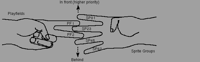
Figure 7-2: Analogy for Video Priority
Five possible positions can be chosen for each of the two "playfield
fingers." For example, you can place playfield 1 on top of sprites 0 and 1
(0), between sprites 0 and 1 and sprites 2 and 3 (1), between sprites 2
and 3 and sprites 4 and 5 (2), between sprites 4 and 5 and sprites 6 and 7
(3), or beneath sprites 6 and 7 (4). You have the same possibilities for
playfield 2.
The numbers 0 through 4 shown in parentheses in the preceding paragraph
are the actual values you use to select the playfield priority positions.
See next section Setting the Priority Control Register .
You can also control the priority of playfield 2 relative to playfield 1.
This gives you additional choices for the way you can design the
screen priorities .
7 / Video Priorities / Setting the Priority Control Register
This register lets you define how objects will pass in front of each other
or hide behind each other. Normally, playfield 1 appears in front of
playfield 2. The PF2PRI bit reverses this relationship, making playfield 2
more important. You control the video priorities by using the bits in
BPLCON2 (for "bitplane control register number 2") as shown in Table
7-1.


                  Table 7-1: Bits in BPLCON2

             Bit
            Number         Name           Function
            ------         ----           --------
             15-7                      Not used (keep at 0)

                6     PF2PRI           Playfield 2 priority

              5-3     PF2P2 - PF2P0    Playfield 2 placement with
                                       respect to the sprites

              2-0     PF1P2 - PF1P0    Playfield 1 placement with
                                       respect to the sprites


The binary values that you give to bits PF1P2-PF1P0 determine where
playfield 1 occurs in the priority chain as shown in Table 7-2. This
matches the description given in the previous section.

   Be careful:
   -----------
   PF2P2 - PF2P0, bits 5-3, are the priority bits for normal (non-dual)
   playfields.


  Table 7-2: Priority of Playfields Based on Values of Bits PF1P2-PF1P0

             Value                 Placement
             -----                 ---------
                    (from most important to least important)

              000     PF1     SP01    SP23    SP45    SP67
              001     SP01    PF1     SP23    SP45    SP67
              010     SP01    SP23    PF1     SP45    SP67
              011     SP01    SP23    SP45    PF1     SP67
              100     SP01    SP23    SP45    SP67    PF1


In this table, PF1 stands for playfield 1, and SP01 stands for the
 group of sprites  numbered 0 and 1. SP23 stands for sprites 2 and 3 as a
group; SP45 stands for sprites 4 and 5 as a group; and SP67 stands for
sprites 6 and 7 as a group.

Bits PF2P2-PF2P0 let you position playfield 2 among the sprite priorities
in exactly the same way. However, it is the PF2PRI bit that determines
which of the two playfields appears in front of the other on the screen.
Here is a sample of possible BPLCON2 register contents that would create
something a little unusual:

              BITS    15-7    PF2PRI  PF2P2-0 PF1P2-0
              VALUE     0s      1       010     000

This will result in a sprite/playfield priority placement of:

                PF1  SP01  SP23  PF2  SP45  SP67

In other words, where objects pass across each other, playfield 1 is in
front of sprite 0 or 1; and sprites 0 through 3 are in front of playfield
2. However, playfield 2 is in front of playfield 1 in any area where they
overlap and where playfield 2 is not blocked by sprites 0 through 3.

Figure 7-3 shows one use of sprite/playfield priority. The single sprite
object shown on the diagram is sprite 0. The sprite can "fly" across
playfield 2, but when it crosses playfield 1 the sprite disappears behind
that playfield. The result is an unusual video effect that causes the
object to disappear when it crosses an invisible boundary on the screen.


    +---------------------+    +---------------------+
    |#####################|    |                     |
    |#####################|    |                     |
    |#####################|    |      ·········      |
    |#####################|    |      ·········      |
    |####                 |    |·····················|         __
    |####                 |    |·····················|        /  \
    |####                 |    |·····················|     __/____\__
    |####                 |    |·····················|    |          |
    |####                 |    |·····················|    |__________|
    |####                 |    |·····················|       \    /
    |####                 |    |·····················|        \__/
    |####                 |    |·····················|
    |#####################|    |      ·········      |      Sprite 0
    |#####################|    |      ·········      |
    |#####################|    |                     |
    |#####################|    |                     |
    +---------------------+    +---------------------+

          Playfield 1                Playfield 2


    +---------------------+
    |#####################|
    |#####################|
    |######·········######|
    |######·-·-·-·-·######|- - - - -
    |···|·__··············|
    |····/  \·············|    When everything is displayed together.
    |···|____\__··········|    sprite 0 is more important than playfield 2
    |····       |·········|    but less important than playfield 1.
    |···|____ __|·········|    So even though you can't see the boundary,
    |····    /············|    the sprite disappears "behind" the
    |···|\__/·············|    invisible PF1 boundary.
    |·····················|
    |######·-·-·-·-·######|- - - - -
    |######·········######|
    |#####################|
    |#####################|
    +---------------------+


                  Figure 7-3: Sprite/Playfield Priority
7 System Control Hardware / Collision Detection
You can use the hardware to detect collisions between one  sprite group
and another  sprite group , any  sprite group  and either of the
playfields, the two playfields, or any combination of these items.

The first kind of collision is typically used in a game operation to
determine if a missile has collided with a moving player. The second kind
of collision is typically used to keep a moving object within specified
on-screen boundaries. The third kind of collision detection allows you to
define sections of playfield as individual objects, which you may move
using the blitter. This is called playfield animation. If one playfield is
defined as the backdrop or playing area and the other playfield is used to
define objects (in addition to the sprites), you can sense collisions
between the playfield-objects and the sprites or between the
playfield-objects and the other playfield.

 How Collisions are Determined
 How To Interpret the Collision Data
 How Collision Detection is Controlled
7 / Collision Detection / How Collisions are Determined
The video output is formed when the input data from all of the bitplanes
and the sprites is combined into a common data stream for the display. For
each of the pixel positions on the screen, the color of the highest
priority object is displayed. Collisions are detected when two or more
objects attempt to overlap in the same pixel position. This will set a bit
in the  collision data register .
7 / Collision Detection / How To Interpret the Collision Data
The collision data register, CLXDAT, is read-only, and its contents are
automatically cleared to 0 after it is read.  Its bits are as shown in
Table 7-3.

                Table 7-3: CLXDAT Bits


          Bit Number      Collisions Registered
          ----------      ---------------------
              15      not used
              14      Sprite 4 (or 5) to sprite 6 (or 7)
              13      Sprite 2 (or 3) to sprite 6 (or 7)
              12      Sprite 2 (or 3) to sprite 4 (or 5)
              11      Sprite 0 (or 1) to sprite 6 (or 7)
              10      Sprite 0 (or 1) to sprite 4 (or 5)
              9       Sprite 0 (or 1) to sprite 2 (or 3)
              8       Even bitplanes to sprite 6 (or 7)
              7       Even bitplanes to sprite 4 (or 5)
              6       Even bitplanes to sprite 2 (or 3)
              5       Even bitplanes to sprite 0 (or 1)
              4       Odd  bitplanes to sprite 6 (or 7)
              3       Odd  bitplanes to sprite 4 (or 5)
              2       Odd  bitplanes to sprite 2 (or 3)
              1       Odd  bitplanes to sprite 0 (or 1)
              0       Even bitplanes to odd bitplanes


   About odd-numbered sprites.
   ---------------------------
   The numbers in parentheses in Table 7-3 refer to collisions that will
   register only if you want them to show up. The
    collision control register  described below lets you either ignore or
   include the odd-numbered sprites in the collision detection.


Notice that in this table, collision detection does not change when you
select either single- or dual-playfield mode. Collision detection depends
only on the actual bits present in the odd-numbered or even-numbered
bitplanes. The  collision control register  specifies how to handle the
bitplanes during collision detect.
7 / Collision Detection / How Collision Detection is Controlled
The collision control register, CLXCON, contains the bits that define
certain characteristics of collision detection. Its bits are shown in
Table 7-4.

                  Table 7-4: CLXCON Bits

    Bit
   Number    Name      Function
   ------    ----      --------
     15      ENSP7     Enable sprite 7 (OR with sprite 6)
     14      ENSP5     Enable sprite 5 (OR with sprite 4)
     13      ENSP3     Enable sprite 3 (OR with sprite 2)
     12      ENSP1     Enable sprite 1 (OR with sprite 0)
     11      ENBP6     Enable bitplane 6 (match required for collision)
     10      ENBP5     Enable bitplane 5 (match required for collision)
     9       ENBP4     Enable bitplane 4 (match required for collision)
     8       ENBP3     Enable bitplane 3 (match required for collision)
     7       ENBP2     Enable bitplane 2 (match required for collision)
     6       ENBP1     Enable bitplane 1 (match required for collision)
     5       MVBP6     Match value for bitplane 6 collision
     4       MVBP5     Match value for bitplane 5 collision
     3       MVBP4     Match value for bitplane 4 collision
     2       MVBP3     Match value for bitplane 3 collision
     1       MVBP2     Match value for bitplane 2 collision
     0       MVBP1     Match value for bitplane 1 collision


Bits 15-12 let you specify that collisions with a sprite pair are to
include the odd-numbered sprite of a pair of sprites.  The even-numbered
sprites always are included in the collision detection. Bits 11-6 let you
specify whether to include or exclude specific bitplanes from the
collision detection. Bits 5-0 let you specify the polarity (true-false
condition) of bits that will cause a collision. For example, you may wish
to register collisions only when the object collides with "something
green" or "something blue." This feature, along with the collision enable
bits, allows you to  specify the exact bits, and their polarity, for the
collision to be registered.

   NOTE:
   -----
   This register is write-only. If all bitplanes are excluded
   (disabled), then a bitplane collision will always be detected.
7 System Control Hardware / Beam Position Detection
Sometimes you might want to synchronize the 680x0 processor to the video
beam that is creating the screen display. In some cases, you may also wish
to update a part of the display memory after the system has already
accessed the data from the memory for the display area.

The address for accessing the beam counter is provided so that you can
determine the value of the video beam counter and perform certain
operations based on the beam position.

   NOTE:
   -----
   The Copper is already capable of watching the display position
   for you and doing certain register-based operations automatically.
   Refer to the  Copper Interrupts  section and
    for further information.

In addition, when you are using a light pen, this same address is used to
read the  light pen position  rather than the beam position. This is
described fully in Chapter 8, "Interface Hardware."

 Using the Beam Position Counter
7 / Beam Position Detection / Using the Beam Position Counter
There are four addresses that access the beam position counter. Their
usage is described in Table 7-5.


          Table 7-5: Contents of the Beam Position Counter


  VPOSR   Read-only   Read the high bit of the vertical position (V8) and
                      the frame-type bit.

          Bit 15      LOF (Long-frame bit). Used to initialize interlaced
                      displays.

          Bits 14-1   Unused

          Bit 0       High bit of the vertical position (V8).  Allows PAL
                      line counts (313) to appear in PAL versions of the
                      Amiga.

  VHPOSR  Read-only   Read vertical and horizontal position of the counter
                      that is producing the beam on the screen (also
                      reads the light pen).

          Bits 15-8   Low bits of the vertical position, bits V7-V0

          Bits  7-0   The horizontal position, bits H8-H1.  Horizontal
                      resolution is 1/160th of the screen width.

  VPOSW   Write only  Bits same as VPOSR above.

  VHPOSW  Write only  Bits same as VHPOSR above.  Used for counter
                      synchronization with chip test patterns.


As usual, the address pairs VPOSR,VHPOSR and VPOSW,VHPOSW can be read from
and written to as long words, with the most significant addresses being
VPOSR and VPOSW.
7 System Control Hardware / Interrupts
This system supports the full range of 680x0 processor interrupts. The
various kinds of interrupts generated by the hardware are brought into the
peripherals chip and are translated into six of the seven available
interrupts of the 680x0.

 Nonmaskable Interrupt                       Interrupt Control Registers
 Maskable Interrupts                         Setting and Clearing Bits
 User Interface to the Interrupt System
7 / Interrupts / Nonmaskable Interrupt
Interrupt level 7 is the nonmaskable interrupt and is not generated
anywhere in the current system. The raw interrupt lines of the 680x0, IPL2
through IPL0, are brought out to the expansion connector and can be used
to generate this  level 7 interrupt  for debugging purposes.
7 / Interrupts / Maskable Interrupts
Interrupt levels 1 through 6  are generated. Control registers within the
peripherals chip allow you to mask certain of these sources and prevent
them from generating a 680x0 interrupt.
7 / Interrupts / User Interface to the Interrupt System
The system software has been designed to correctly handle all system
hardware interrupts at levels 1 through 6. A separate set of input
lines, designated INT2* and INT6* have been routed to the expansion
connector for use by external hardware for interrupts. These are known as
the external low- and external high-level interrupts.

These interrupt lines are connected to the peripherals chip and create
 interrupt levels 2 and 6 , respectively. It is recommended that you take
advantage of the interrupt handlers built into the operating system by
using these external interrupt lines rather than generating interrupts
directly on the processor interrupt lines.
7 / Interrupts / Interrupt Control Registers
There are two interrupt registers, interrupt enable (mask) and interrupt
request (status). Each register has both a read and a write address.  The
names of the interrupt addresses are:

    INTENA
      Interrupt0 enable (mask) - write only. Sets or clears specific
      bits of INTENA.

    INTENAR
      Interrupt enable (mask) read - read only. Reads contents of INTENA.

    INTREQ
      Interrupt request (status) - write only. Used by the processor
      to force a certain kind of interrupt to be processed (software
      interrupt). Also used to clear interrupt request flags once the
      interrupt process is completed.

    INTREQR
      Interrupt request (status) read - read only. Contains the bits
      that define which items are requesting interrupt service.

      The bit positions in the interrupt request register correspond
      directly to those same positions in the interrupt enable
      register. The only difference between the read-only and the
      write-only addresses shown above is that  bit 15  has no meaning
      in the read-only addresses.
7 / Interrupts / Setting and Clearing Bits
Below are the meanings of the bits in the interrupt control registers and
how you use them.

 Set and Clear                    Audio Interrupts
 Master Interrupt Enable          Blitter Interrupt
 External Interrupts              Disk Interrupt
 Vertical Blanking Interrupt      Serial Port Interrupts
 Copper Interrupt


     Figure 7-4: Interrupt Priorities
7 / / Setting and Clearing Bits / Set and Clear
The  interrupt registers , as well as the  DMA control register , use a
special way of selecting which of the bits are to be set or cleared. Bit
15 of these registers is called the SET/CLR bit.

When you wish to set a bit (make it a 1), you must place a 1 in the
position you want to set and a 1 into position 15.

When you wish to clear a bit (make it a 0), you must place a 1 in the
position you wish to clear and a 0 into position 15.

Positions 14-0 are bit selectors. You write a 1 to any one or more bits to
select that bit. At the same time you write a 1 or 0 to bit 15 to either
set or clear the bits you have selected. Positions 14-0 that have 0 value
will not be affected when you do the write. If you want to set some bits
and clear others, you will have to write this register twice (once for
setting some bits, once for clearing others).
7 / / Setting and Clearing Bits / Master Interrupt Enable
Bit 14 of the  interrupt registers  (INTEN) is for interrupt enable. This
is the master interrupt enable bit. If this bit is a 0, it disables all
other interrupts. You may wish to clear this bit to temporarily disable
all interrupts to do some critical processing task.

   Warning:
   --------
   This bit is used for enable/disable only. It creates no interrupt
   request.
7 / / Setting and Clearing Bits / External Interrupts
Bits 13 and 3 of the  interrupt registers  are reserved for external
interrupts.

Bit 13, EXTER, becomes a 1 when the system line called INT6* becomes a
logic 0. Bit 13 generates a  level 6 interrupt .

Bit 3, PORTS, becomes a 1 when the system line called INT2* becomes a
logic 0. Bit 3 causes a  level 2 interrupt .
7 / / Setting and Clearing Bits / Vertical Blanking Interrupt
Bit 5, VERTB, causes an interrupt at line 0 (start of vertical blank) of
the video display frame. The system is often required to perform many
different tasks during the vertical blanking interval. Among these tasks
are the updating of various pointer registers, rewriting lists of Copper
tasks when necessary, and other system-control operations.

The minimum time of vertical blanking is 20 horizontal scan lines for an
NTSC system and 25 horizontal scan lines for a PAL system. The range
starts at line 0 and ends at line 20 for NTSC or line 25 for PAL. After
the minimum vertical blanking range, you can control where the display
actually starts by using the  DIWSTRT  (display window start) register
to extend the effective vertical blanking time. See Chapter 3, "Playfield
Hardware," for more information on  DIWSTRT .

If you find that you still require additional time during vertical
blanking, you can use the Copper to create a  level 3 interrupt . This
Copper interrupt would be timed to occur just after the last line of
display on the screen (after the display window stop which you have
defined by using the  DIWSTOP  register).
7 / / Setting and Clearing Bits / Copper Interrupt
Bit 4, COPER, is used by the Copper to issue a  level 3 interrupt . The
Copper can change the content of any of the bits of this register, as it
can write any value into most of the machine registers. However, this bit
has been reserved for specifically identifying the Copper as the interrupt
source.

Generally, you use this bit when you want to sense that the display beam
has reached a specific position on the screen, and you wish to change
something in memory based on this occurrence.
7 / / Setting and Clearing Bits / Audio Interrupts
Bits 10 - 7, AUD3 - 0, are assigned to the audio channels. They are called
AUD3, AUD2, AUD1, and AUD0 and are assigned to channels 3, 2, 1, and 0,
respectively.

This  level 4 interrupt  signals "audio block done." When the audio DMA is
operating in  automatic mode , this interrupt occurs when the last word in
an audio data stream has been accessed. In  manual mode , it occurs when
the  audio data register  is ready to accept another word of data.

See Chapter 5, "Audio Hardware," for more information about
 interrupt generation and timing .
7 / / Setting and Clearing Bits / Blitter Interrupt
Bit 6, BLIT, signals "blitter finished." If this bit is a 1, it indicates
that the blitter has completed the requested data transfer. The blitter is
now ready to accept another task. This bit generates a  level 3 interrupt .
7 / / Setting and Clearing Bits / Disk Interrupt
Bits 12 and 1 of the  interrupt registers  are assigned to disk interrupts.

Bit 12, DSKSYN, indicates that the  sync register  matches disk data. This
bit generates a  level 5 interrupt .

Bit 1, DSKBLK, indicates "disk block finished." It is used to indicate
that the specified disk DMA task that you have requested has been
completed. This bit generates a  level 1 interrupt .

More information about disk data transfer and  interrupts  may be found
in Chapter 8, "Interface Hardware."
7 / / Setting and Clearing Bits / Serial Port Interrupts
The following serial interrupts are associated with the specified bits of
the  interrupt registers .

Bit 11, RBF (for receive buffer full), specifies that the input buffer of
the UART has data that is ready to read. This bit generates a
 level 5 interrupt .

Bit 0, TBE (for "transmit buffer empty"), specifies that the output
buffer of the UART needs more data and data can now be written into this
buffer. This bit generates a  level 1 interrupt .
7 / / Setting and Clearing Bits / Figure 7-4: Interrupt Priorities
               Exec
Hardware     Software
Priority     Priority     Description                  Name
--------     --------     -----------                  ----
           ____
          |     1         transmitter buffer empty     TBE
          |
   1 -----|     2         disk block complete          DSKBLK
          |
          |     3         software interrupt           SOFTINT
          |----
   2 -----|     4         external INT2 & CIAA         PORTS
          |----
          |     5         graphics coprocessor         COPER
          |
   3 -----|     6         vertical blank interval      VERTB
          |
          |     7         blitter finished             BLIT
          |----
          |     8         audio channel 2              AUD2
          |
          |     9         audio channel 0              AUD0
   4 -----|
          |     10        audio channel 3              AUD3
          |
          |     11        audio channel 1              AUD1
          |----
          |     12        receiver buffer full         RBF
   5 -----|
          |     13        disk sync pattern found      DSKSYNC
          |----
          |     14        external INT6 & CIAB         EXTER
   6 -----|
          |     15        special (master enable)      INTEN
          |----
   7 -----|____ --        non-maskable interrupt       NMI
7 System Control Hardware / DMA Control
Many different direct memory access (DMA) functions occur during system
operation. There is a read address as well as a write address to the DMA
control register so you can tell which DMA channels are enabled.

The address names for the DMA registers are as follows:

   DMACONR - Direct Memory Access Control - read-only.
   DMACON  - Direct Memory Access Control - write-only.

The contents of this register are shown in Table 7-6 (bit on if enabled).


   Bit
  Number     Name      Function
  ------     ----      --------
    15      SET/CLR    The set/reset control bit. See
                        description of bit 15 .


    14      BBUSY      Blitter busy status - read-only

    13      BZERO      Blitter zero status - read-only. Remains 1 if,
                       during a blitter operation, the blitter output
                       was always zero.

    12, 11             Unassigned

    10      BLTPRI     Blitter priority.  Also known as "blitter-nasty."
                       When this is a 1, the blitter has full (instead
                       of partial) priority over the 680x0.

    9       DMAEN      DMA enable.  This is a master DMA enable bit.
                       It enables the DMA for all of the channels at
                       bits 8-0.

    8       BPLEN      Bitplane DMA enable

    7       COPEN      Coprocessor DMA enable

    6       BLTEN      Blitter DMA enable

    5       SPREN      Sprite DMA enable

    4       DSKEN       Disk DMA enable

    3-0     AUDxEN     Audio DMA enable for channels 3-0 (x = 3 - 0).


            Table 7-6: Contents of DMA Control Register


For more information on using the DMA, see the following chapters:

   Copper     Chapter 2: Coprocessor Hardware
   Bitplanes  Chapter 3: Playfield Hardware
   Sprites    Chapter 4: Sprite Hardware
   Audio      Chapter 5: Audio Hardware
   Blitter    Chapter 6: Blitter Hardware
   Disk       Chapter 8: Interface Hardware

Processor Access To Chip Memory
-------------------------------
The Amiga chips access Chip memory directly via DMA, rather than utilizing
traditional bus arbitration mechanisms. Therefore, processor supplied
features for multiprocessor support, such as the 68000 TAS (test and set)
instruction, cannot serve their intended purpose and are not supported by
the Amiga architecture.
7 System Control Hardware / Reset and Early Startup Operation
When the Amiga is turned on or externally reset, the memory map is in a
special state.  An additional copy of the system ROM responds starting at
memory location $00000000.  The system RAM that would normally be located
at this address is not available.  On some Amiga models, portions of the
RAM still respond.  On other models, no RAM responds.  Software must
assume that memory is not available.  The OVL bit in one of the 8520 Chips
disables the overlay (See  Appendix F  for the bit location).

The Amiga System ROM contains an ID code as the first word.  The value of
the ID code may change in the future.  The second word of the ROM contains
a JMP instruction ($4ef9).  The next two words are used as the initial
program counter by the 680x0 processor.

The 68000 RESET instruction works much like external reset or power on.
All memory and AUTOCONFIG(TM) cards disappear, and the ROM image appears
at location $00000000.  The difference is that the CPU continues execution
with the next instruction.  Since RAM may not be available, special care
is needed to write reboot code that will reliably reboot all Amiga models.

     coldreboot.asm
Converted on 22 Apr 2000 with RexxDoesAmigaGuide2HTML 2.1 by Michael Ranner.