Amiga® Hardware Reference Manual: 8 Interface Hardware
This chapter covers the interface hardware through which the Amiga talks
to the outside world, including the following features:

  * Two multiple purpose mouse/joystick/light pen control ports
  * Disk controller (for floppy disk drives & other MFM and GCR devices)
  * Keyboard
  * Centronics compatible parallel I/O interface (for printers)
  * RS232-C compatible serial interface (for external modems or other
      serial devices)
  * Video output connectors (RGB, monochrome, NTSC, RF modulator, video
      slot)

 Controller Port Interface      Serial I/O Interface
 Floppy Disk Controller         Parallel I/O Interface
 The Keyboard                   Display Output Connections
8 Interface Hardware / Controller Port Interface
Each Amiga has two nine-pin connectors that can be used for input or
output with a variety of controllers. Usually, the nine-pin connectors
are used with a mouse or joystick but they will also accept input from
light pens, paddles, trackballs, and other popular input devices.
Figure 8-1 shows one of the two connectors and the corresponding face-on
view of a standard controller plug, while table 8-1 gives the pin
assignments for some typical controllers.
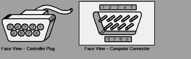
Figure 8-1: Controller Plug and Computer Connector
Table 8-1: Typical Controller Connections
Mouse,
Trackball, Proportional X-Y
Driving Controller Proportional
Pin Joystick Controller (Pair) Joystick Light Pen
--- -------- ---------- ------------ ------------ ---------
1 Forward V-pulse --- Button 3** ---
2 Back H-pulse --- --- ---
3 Left VQ-pulse Left button Button 1 ---
4 Right HQ-pulse Right button Button 2 ---
5* --- Middle Right POT POT X Pen pressed
button** to screen
6* Button 1 Left button --- --- Beam trigger
7 --- +5V +5V +5V +5V
8 GND GND GND GND GND
9* Button 2** Right button Left POT POT Y Button 2**
* These pins may also be configured as outputs
** These buttons are optional
Registers Used with the Controller Port
Reading Mouse/Trackball Controllers
Reading Digital Joystick Controllers
Reading Proportional Controllers
Reading a Light Pen
Digital I/O on the Controller Port
8 / Controller Port Interface / Registers used with Controller Port
The Amiga chip registers that handle the  controller port  I/O are listed
below.

   JOY0DAT  ($DFF00A)  Counter for digital (mouse) input (port 1)
   JOY1DAT  ($DFF00C)  Counter for digital (mouse) input (port 2)
   CIAAPRA  ($BFE001)  Input and output for pin 6 (port 1 & 2 fire buttons)
   POT0DAT  ($DFF012)  Counter for proportional input (port 1)
   POT1DAT  ($DFF014)  Counter for proportional input (port 2)
   POTGO    ($DFF034)  Write proportional pin values and start counters
   POTGOR   ($DFF016)  Read proportional pin values
   BPLCON0  ($DFF100)  Bit 3  enables the light pen  latch
   VPOSR    ($DFF004)  Read  light pen position  (high order bits)
   VHPOSR   ($DFF006)  Read  light pen position  (low order bits)
8 / Controller Port Interface / Reading Mouse/Trackball Controllers
Pulses entering the mouse inputs are converted to separate horizontal and
vertical counts.  The 8 bit wide horizontal and vertical
 counter registers  can track mouse movement without processor
intervention.

The mouse uses quadrature inputs.  For each direction, a mechanical wheel
inside the mouse will produce two pulse trains, one 90 degrees out of
phase with the other (see Figure 8-2 for details).  The phase relationship
determines direction.


  Case 1: Count Up:
          ________            ________            ________            __
         /        \          /        \          /        \          /
  V  ___/          \________/          \________/          \________/
               ________            ________            ________
              /        \          /        \          /        \
  VQ ________/          \________/          \________/          \_______
          ___       ___       ___       ___       ___       ___       __
         /   \     /   \     / 1 \  0  /   \     /   \     /   \     /
  D0 ___/     \___/     \___/     \___/     \___/     \___/     \___/
     ________            ________            ________            _______
             \          /      1 \  0       /        \          /
  D1          \________/          \________/          \________/


  Case 2: Count Down:
          ________            ________            ________            __
         /        \          /        \          /        \          /
  V  ___/          \________/          \________/          \________/
     ________            ________            ________            _______
             \          /        \          /        \          /
  VQ          \________/          \________/          \________/
     ___       ___       ___       ___       ___       ___       ___
        \     /   \     /   \     /   \     /   \     /   \     /   \
  D0     \___/     \___/     \___/     \___/     \___/     \___/     \__
               ________            ________            ________
              /        \          /        \          /        \
  D1 ________/          \________/          \________/          \_______
          ___
             \
  D2          \___ etc           V    VQ   :   D1   D0
                                 ---------------------
                                 0    0    :    1    0
                                 0    1    :    0    1
                                 1    0    :    1    1
                                 1    1    :    0    0


                       Figure 8-2: Mouse Quadrature


The counters increment when the mouse is moved to the right or "down"
(toward you).

The counters decrement when the mouse is moved to the left or "up" (away
from you).

 Reading the Counters
 Counter Limitations
 Mouse Buttons
8 / / Reading Mouse/Trackball Controllers / Reading the Counters
The mouse/trackball counter contents can be accessed by reading register
addresses named  JOY0DAT and JOY1DAT .  These registers contain counts for
ports 1 and 2 respectively.

The contents of each of these 16-bit registers are as follows:

   Bits 15-8     Mouse/trackball vertical count
   Bits  7-0     Mouse/trackball horizontal count
8 / / Reading Mouse/Trackball Controllers / Counter Limitations
These  counters  will "wrap around" in either the positive or negative
direction. If you wish to use the mouse to control something that is
happening on the screen, you must read the  counters  at least once each
 vertical blanking  period and save the previous contents of the
registers. Then you can subtract from the previous readings to determine
direction of movement and speed.

The mouse produces about 200 count pulses per inch of movement in either a
horizontal or vertical direction.  Vertical blanking  happens once each
1/60th of a second. If you read the mouse once each  vertical blanking
period, you will most likely find a count difference (from the previous
count) of less than 127. Only if a user moves the mouse at a speed of more
than 38 inches per second will the  counter  values wrap.  Fast-action
games may need to read the mouse register twice per frame to prevent
 counter  overrun.

If you subtract the current count from the previous count, the absolute
value of the difference will represent the speed. The sign of the
difference (positive or negative) lets you determine which direction the
mouse is traveling.

The easiest way to calculate mouse velocity is with 8-bit signed
arithmetic. The new value of a  counter  minus the previous value will
represent the number of mouse counts since the last check. The example
shown in Table 8-2 presents an alternate method.  It treats both counts as
unsigned values, ranging from 0 to 255.  A count of 100 pulses is measured
in each case.


         Table 8-2: Determining the Direction of the Mouse

                Previous    Current
                 Count       Count     Direction
                --------    -------    ---------
                  200         100      Up (Left)
                  100         200     Down (Right)
                  200          45       Down *
                   45         200        Up **


   Notes for Table 8-2:

   *  Because 200-45 = 155, which is more than 127, the true count must
      be 255 - ( 200-45) = 100; the direction is down.

   ** 45 - 200 = -155.  Because the absolute value of -155 exceeds 127,
      the true count must be  255 + (-155) = 100; the direction is up.
8 / / Reading Mouse/Trackball Controllers / Mouse Buttons
There are two buttons on the standard Amiga mouse. However, the control
circuitry and software support up to three buttons.

   *  The left button on the Amiga mouse is connected to  CIAAPRA
      ($BFE001). Port 1 uses bit 6 and port 2 uses bit 7. A logic
      state of 1 means "switch open." A logic state of 0 means "switch
      closed." (See  Appendix F  for more information.)

   *  Button 2 (right button on Amiga mouse) is connected to pin 9 of
      the  controller ports , one of the proportional pins.  See
       Digital Input/Output on the Controller Port  for details.

   *  Button 3, when used, is connected to pin 5, the other
      proportional  controller input .
8 / Controller Port Interface / Reading Digital Joystick Controllers
Digital joysticks contain four directional switches. Each switch can be
individually activated by the control stick. When the stick is pressed
diagonally, two adjacent switches are activated. The total number of
possible directions from a digital joystick is 8. All digital joysticks
have at least one fire button.
Digital joystick switches are of the normally open type. When the
switches are pressed, the input line is shorted to ground. An open switch
reads as "1", a closed switch as "0".
Reading the joystick input data logic states is not so simple, however,
because the data registers for the joysticks are the same as the counters
that are used for the mouse or trackball controllers. The joystick
registers are named JOY0DAT and JOY1DAT .
Table 8-3 shows how to interpret the data once you have read it from these
registers. The true logic state of the switch data in these registers is
"1 = switch closed."
Data Bit Interpretation
-------- --------------
1 True logic state of "right" switch.
9 True logic state of "left" switch.
1 (XOR) 0 You must calculate the exclusive-or of bits 1 and 0
to obtain the logic state of the "back" switch.
9 (XOR) 8 You must calculate the exclusive-or of bits 9 and 8
to obtain the logic state of the "forward" switch.
Table 8-3: Interpreting Data from JOY0DAT and JOY1DAT
The fire buttons for ports 0 and 1 are connected to bits 6 and 7 of
CIAAPRA ($BFE001). A 0 here indicates the switch is closed.
Some, but not all, joysticks have a second button. We encourage the use
of this button if the function the button controls is duplicated via the
keyboard or another mechanism. This button may be read in the same manner
as the right mouse button .
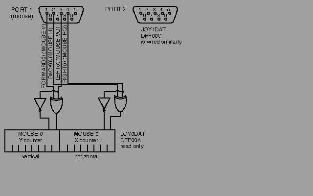
Figure 8-3: Joystick to Counter Connections
8 / Controller Port Interface / Reading Proportional Controllers
Each of the game  controller ports  can handle two variable-resistance
input devices, also known as proportional input devices. This section
describes how the positions of the proportional input devices can be
determined. There are two common types of proportional controllers:  the
"paddle" controller pair and the X-Y proportional joystick. A paddle
controller pair consists of two individual enclosures, each containing a
single resistor and fire-button and each connected to a common
 controller port  input connector. Typical connections are shown in Figure
8-4.

    LEFT PADDLE                          RIGHT PADDLE

          resistive element                    resistive element

     ____/\  /\  /\  /\  /\____           ____/\  /\  /\  /\  /\____
    |      \/  \/  \/  \/                |      \/  \/  \/  \/
    |+5           ^                      |+5           ^
    |             |_ _ _ _ _ _           |             |_ _ _ _ _ _
                              |                                    |
  pin 7                     pin 9      pin 7                     pin 9


    |                         |          |                         |
    |<- - - fire button - - ->|          |<- - - fire button - - ->|
    |                         |          |                         |

  pin 8                     pin 3      pin 8                     pin 3


                Figure 8-4: Typical Paddle Wiring Diagram


In an X-Y proportional joystick, the resistive elements are connected
individually to the X and Y axes of a single controller stick.

 Reading Proportional Controller Buttons
 Interpreting Proportional Controller Position
 Proportional Controller Registers
 Potentiometer Specifications
8 / / Reading Controllers / Reading Proportional Controller Buttons
For the paddle controllers, the left and right joystick direction lines
serve as the fire buttons for the left and right paddles.
8 / / Reading Controllers / Interpreting Controller Position
Interpreting the position of the proportional controller normally requires
some preliminary work during the vertical blanking interval.
During vertical blanking , you write a value into an address called
POTGO . For a standard X-Y joystick, this value is hex 0001. Writing to
this register starts the operation of some special hardware that reads the
potentiometer values and sets the values contained in the POT registers
(described below) to zero.
The read circuitry stays in a reset state for the first seven or eight
horizontal video scan lines. Following the reset interval, the circuit
allows a charge to begin building up on a timing capacitor whose charge
rate will be controlled by the position of the external controller
resistance. For each horizontal scan line thereafter, the circuit compares
the charge on the timing capacitor to a preset value. If the charge is
below the preset, the POT counter is incremented. If the charge is above
the preset, the counter value will be held until the next POTGO is
issued.
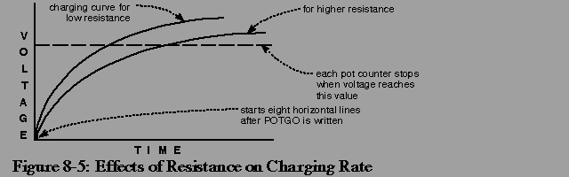
Figure 8-5: Effects of Resistance on Charging Rate
You normally issue POTGO at the beginning of a video screen, then read
the values in the during the next vertical blanking
period, just before issuing POTGO again.
Nothing in the system prevents the counters from overflowing (wrapping
past a count of 255). However, the system is designed to insure that the
counter cannot overflow within the span of a single screen. This allows
you to know for certain whether an overflow is indicated by the controller.
8 / / Reading Controllers / Proportional Controller Registers
The following registers are used for the proportional controllers:

   POT0DAT  - port 1 data (vertical/horizontal)
   POT1DAT  - port 2 data (vertical/horizontal)

   Bit positions:

   Bits 15-8   POT0Y value or POT1Y value
   Bits 7-0    POT0X value or POT1X value

All counts are reset to zero when  POTGO  is written with bit zero high.
Counts are normally read one frame after the scan circuitry is enabled.
8 / / Reading Proportional Controllers / Potentiometer Specifications
The resistance of the potentiometers should be a linear taper. Based on
the design of the integrating analog-to-digital converter used, the
maximum resistance should be no more than 528K (470K +/- 10 percent is
suggested) for either the X or Y pots. This is based on a charge capacitor
of 0.047uf, +/- 10 percent, and a maximum time of 16.6 milliseconds for
charge to full value, ie. one video frame time.
All potentiometers exhibit a certain amount of "jitter". For acceptable
results on a wide base of configurations, several input readings will need
to be averaged.
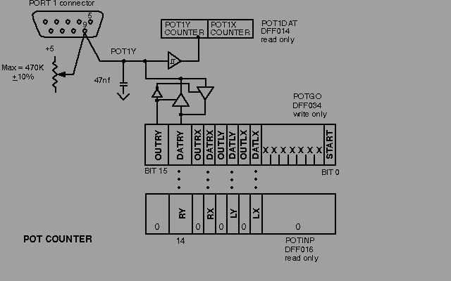
Figure 8-6: Potentiometer Charging Circuit
8 / Controller Port Interface / Reading A Light Pen
A light pen can be connected to one of the  controller ports . On the
A1000, the light pen must be connected to port 1. Changing ports requires
a minor internal modification. On the A500, A2000 and A3000 the default is
port 2. An internal jumper can select port 1.  Regardless of the port
used, the light pen design is the same.

The signal called "pen-pressed-to-screen" is typically actuated by a
switch in the nose of the light pen. Note that this switch is connected to
one of the potentiometer inputs and must be read as same as the right or
middle  mouse button .

The principles of light pen operation are as follows:

   1. Just as the system exits  vertical blank , the capture circuitry
      for the light pen is automatically enabled.

   2. The video beam starts to create the picture, sweeping from left
      to right for each horizontal line as it paints the picture from
      the top of the screen to the bottom.

   3. The sensors in the light pen see a pulse of light as the video
      beam passes by. The pen converts this light pulse into an
      electrical pulse on the "Beam Trigger" line (pin 6).

   4. This trigger signal tells the internal circuitry to capture and
      save the current contents of the beam register,  VPOSR . This
      allows you to determine where the pen was placed by reading the
      exact horizontal and vertical value of the counter beam at the
      instant the beam passed the light pen.

 Reading the Light Pen Registers
8 / / Reading A Light Pen / Reading the Light Pen Registers
The light pen register is at the same address as the beam counters. The
bits are as follows:

   VPOSR:     Bit 15       Long frame/short frame.  0=short frame
              Bits 14-1    Chip ID code.  Do not depend on value!
              Bit 0        V8 (most significant bit of vertical position)

   VHPOSR:    Bits 15-8    V7-V0 (vertical position)
              Bits 7-0     H8-H1 (horizontal position)

The software can refer to this register set as a long word whose address
is VPOSR.

The positional resolution of these registers is as follows:

   Vertical      1 scan line in non-interlaced mode
                 2 scan lines in interlaced mode (However, if you know
                 which interlaced frame is under display, you can
                 determine the correct position)

   Horizontal    2 low resolution pixels in either high or low resolution

The quality of the light pen will determine the amount of short-term
jitter.  For most applications, you should average several readings
together.

To enable the light pen input, write a 1 into bit 3 (LPEN) of  BPLCON0 .
Once the light pen input is enabled and the light pen issues a trigger
signal, the value in VPOSR is frozen. If no trigger is seen, the counters
latch at the end of the display field. It is impossible to read the
current beam location while the VPOSR register is latched. This freeze is
released at the end of internal  vertical blanking  (vertical position
20). There is no single bit in the system that indicates a light pen
trigger. To determine if a trigger has occurred, use one of these methods:

   1. Read (long) VPOSR twice.

   2. If both values are not the same, the light pen has not triggered
      since the last top-of-screen (V = 20).

   3. If both values are the same, mask off the upper 15 bits of the
      32-bit word and compare it with the hex value of $10500 (V = 261).

   4. If the VPOSR value is greater than $10500, the light pen has not
      triggered since the last top-of-screen. If the value is less,
      the light pen has triggered and the value read is the screen
      position of the light pen.

A somewhat simplified method of determining the truth of the light pen
value involves instructing the system software to read the register only
during the internal  vertical blanking  period of 0 < V20:

   1. Read (long) VPOSR once, during the period of 0 < V20.

   2. Mask off the upper 15 bits of the 32-bit word and compare it
      with the hex value of $10500 (V = 261).

   3. If the VPOSR value is greater than $10500, the light pen has not
      triggered since the last top-of-screen. If the value is less,
      the light pen has triggered and the value read is the screen
      position of the light pen.

Note that when the light pen latch is enabled, the VPOSR register may be
latched at any time, and cannot be relied on as a counter.  This behavior
may cause problems with software that attempts to derive timing based on
VPOSR ticks.
8 / Controller Port Interface / Digital I/O On The Controller Port
The Amiga can read and interpret many different and nonstandard
controllers. The control lines built into the POTGO register (address
$DFF034) can redefine the functions of some of the  controller port  pins.

Table 8-4 is the POTGO register bit description. POTGO ($DFF034) is the
write-only address for the pot control register. POTGOR (formerly POTINP)
($DFF016) is the read-only address for the pot control register. The
pot-control register controls a four-bit bidirectional I/O port that
shares the same four pins as the four pot inputs.


     Table 8-4: POTGO ($DFF034) and POTGOR ($DFF016) Registers

       Bit
       Number  Name    Function
       ------  ----    --------
       15      OUTRY   Output enable for bit 14 (1=output)
       14      DATRY   data for port 2, pin 9
       13      OUTRX   Output enable for bit 12
       12      DATRX   data for port 2, pin 5
       11      OUTLY   Output enable for bit 10
       10      DATLY   data for port 1, pin 9 (right  mouse button )
       09      OUTLX   Output enable for bit 8
       08      DATLX   data for port 1, pin 5 (middle  mouse button )
       07-01   X       chip revision identification number
       00      START   Start pots (dump capacitors, start counters)


Instead of using the pot pins as variable-resistive inputs, you can use
these pins as a four-bit input/output port.  This provides you with two
additional pins on each of the two  controller ports  for general purpose
I/O.

If you set the output enable for any pin to a 1, the Amiga disconnects the
potentiometer control circuitry from the port, and configures the pin for
output.  The state of the data bit controls the logic level on the output
pin.  This register must be written to at the POTGO address, and read
from the POTGOR address. There are large capacitors on these lines, and
it can take up to 300 microseconds for the line to change state.

To use the entire register as an input, sensing the current state of the
pot pins, write all 0s to POTGO.  Thereafter you can read the current
state by using read-only address POTGOR.  Note that bits set as inputs
will be connected to the proportional counters (See the description of the
START bit in POTGO).

These lines can also be used for button inputs.  A button is a normally
open switch that shorts to ground.  The Amiga must provide a pull-up
resistance on the sense pin.  To do this, set the proper pin to output,
and drive the line high (set both OUT... and DAT... to 1).  Reading
POTGOR will produce a 0 if the button is pressed, a 1 if it is not.

The joystick fire buttons can also be configured as outputs.   CIAADDRA
($BFE201) contains a mask that corresponds one-to-one with the data read
register,  CIAAPRA  ($BFE001). Setting a 1 in the direction position makes
the corresponding bit an output.  See Appendix F for more details.
8 Interface Hardware / Floppy Disk Controller
The built-in disk controller in the system can handle up to four MFM-type
devices.  Typically these are double-sided, double-density, 3.5" (90mm) or
5.25" disk drives.  One 3.5" drive is installed in the basic unit.

The controller is extremely flexible.  It can DMA an entire track of raw
MFM data into memory in a single disk revolution.  Special registers allow
the CPU to synchronize with specific data, or read input a byte at a time.
The controller can read and write virtually any double-density MFM encoded
disk, including the Amiga V1.0 format, IBM PC (MS-DOS) 5.25", IBM PC
(MS-DOS) 3.5" and most CP/M (TM) formatted disks.  The controller has
provisions for reading and writing most disk using the Group Coded
Recording (GCR) method, including Apple II (TM) disks.  With motor speed
tricks, the controller can read and write Commodore 1541/1571 format
diskettes.

 Registers Used by the Disk Subsystem
 Disk Subsystem Timing
 Disk Interrupts
8 / Floppy Disk Controller / Registers Used by the Disk Subsystem
The disk subsystem uses two ports on the system's  8520 CIA  chips, and
several registers in the Paula chip:

   CIAAPRA    ($BFE001)    four input bits for disk sensing
   CIABPRB    ($BFD100)    eight output bits for disk selection, control
                             and stepping
   ADKCON     ($DFF09E)    control bits (write only register)
   ADKCONR    ($DFF010)    control bits (read only register)
   DSKPTH     ($DFF020)    DMA pointer (32 bits)
   DSKLEN     ($DFF024)    length of DMA
   DSKBYTR    ($DFF01A)    Disk data byte and status read
   DSKSYNC    ($DFF07E)    Disk sync finder; holds a match word
8 / Floppy Disk Controller / Disk Subsystem Timing
Figures 8-7, 8-8 and 8-9 show the timing parameters of the Amiga's floppy
disk subsystem with a Chinon drive. Keep in mind that this information can
change with floppy drives from other vendors.  To ensure compatibility
with future versions of the system, you should avoid using this
information in applications.


             500ms min
           |<--------->|
         __            |
  MOTOR    |           |
  ON       |___________________________________________________________

         __            |                                       ________
  DRIVE    |           |                                      |
  SELECT   |__________________________________________________|

           |           |                         1.2ms min    |
           |           |                    |<--------------->|
         _____    ___________________________________    ______________
  STEP        |  |                                   |  |
           |  |__|     |                    |        |__|
           |           |                    |
           |  -->|     |<--18ms min         | 1.3ms min |
        -->|           |<--1us min          |<--------->|
         ______________                      __________________________
  WRITE                |                    |
  GATE                 |____________________|
                                               1.2ms min
                 -->|  |<--1000us min       |<---------->|
         ___________   |   (see text)       |             _____________
  SIDE              |  |                    |            |
  SELECT            |____________________________________|

             8us max-->|  |<--        -->|  |<--8us max
         ______________________________________________________________
  WRITE                   |  |  |  |  |  |
  DATA                 |  |__|__|__|__|__|  |


                 Figure 8-7: Chinon Write Timing Diagram

         ____                                                   _______
  DRIVE      |                                                 |
  SELECT     |_________________________________________________|

             |      |            |      | 3ms  |            |  |
             |  t   | 18 ms min  |      | min  | 18 ms min  |  |
             |<---->|<---------->|      |<---->|<---------->|  |<-t
         ________    _________    ___    ___    _________    __________
  STEP           |  |         |  |   |  |   |  |         |  |
                 |__|         |__|   |__|   |__|         |__|

              |  t  |  t  |  t   |   |  |      |  t  |  t   |
              |<--->|<--->|<---->| ->|  |<-t   |<--->|<---->|
               ___________       |                    _________________
  DIRECTION   |           |      |                   |
  SELECT _____|     |     |__________________________|
                    | 4ms
                    | max  |     |  |
                    |<---->|   ->|  |<-t
         __________________          __________________________________
                           |        |
  TRACK 00                 |________|


                 Figure 8-8: Chinon Access Timing Diagram

         __
  DRIVE    |
  SELECT   |___________________________________________________________

        -->|     |<--1us min
         _____    _____________________________________________________
  STEP        |  |
           |  |__|
           |         18ms min
           |     |<------------->|
           |     |   1us min     |
           |<------------------->|
         ________________________         _____________________________
  WRITE                          |       |
  GATE     |     |               |_______|
           |     | 1000us min  |             1.2ms min
           |     | (see text)->| |<--    |<------------>|
         ______________________  |       |               ______________
  SIDE                         |         |              |
  SELECT   |  -->|  |<--18ms   |________________________|
           |     |  |    max
           |1us min |                    |  |           |  |  1000us min
           |<------>|        1.2ms max-->|  |<--     -->|  |<-(see text)
         ______________________________________________________________
  VALID             |  |  |  |              |  |  |  |  |  |  |  |  |  |
  READ DATA         |__|__|__|              |__|__|__|__|  |__|__|__|__|


                  Figure 8-8: Chinon Read Timing Diagram


 CIAAPRA/CIABPRB - Disk selection, control and sensing
 Disk DMA Channel Control
 DSKPTH - Pointer to Data
 DSKLEN - Length, Direction, DMA Enable
 DSKBYTR - Disk Data Byte and Status Read (read-only)
 ADKCON and ADKCONR - Audio and Disk Control Register
 DSKSYNC - Disk Input Synchronizer
8 / / Disk Timing / CIAAPRA/PRB - Disk selection, control and sensing
The following table lists how 8520 chip bits used by the disk subsystem.
Bits labeled  PA  are input bits in CIAAPRA ($BFE001).  Bits labeled
 PB  are output bits located in CIAAPRB ($BFD100).  More information on
how the 8520 chips operate can be found in Appendix F.


                   Table 8-5: Disk Subsystem

Bit   Name         Function
---   ----         --------
PA5   DSKRDY*      Disk ready (active low). The drive will pull this line
                   low when the motor is known to be rotating at full
                   speed.  This signal is only valid when the motor is ON,
                   at other times configuration information may obscure
                   the meaning of this input.

PA4   DSKTRACK0*   Track zero detect.  The drive will pull this line low
                   when the disk heads are positioned over track zero.
                   Software must not attempt to step outwards when this
                   signal is active.  Some drives will refuse to step,
                   others will attempt the step, possibly causing
                   alignment damage.  All new drives must refuse to step
                   outward in this condition.

PA3   DSKPROT*     Disk is write protected (active low).

PA2   DSKCHANGE*   Disk has been removed from the drive.  The signal goes
                   low whenever a disk is removed.  It remains low until
                   a disk is inserted AND a step pulse is received.
      ---------

PB7   DSKMOTOR*    Disk motor control (active low).  This signal is
                   nonstandard on the Amiga system.  Each drive will latch
                   the motor signal at the time its select signal turns
                   on.  The disk drive motor will stay in this state until
                   the next time select turns on.  DSKMOTOR* also controls
                   the activity light on the front of the disk drive.

                   All software that selects drives must set up the motor
                   signal before selecting any drives.  The drive will
                   "remember" the state of its motor when it is not
                   selected.  All drive motors turn off after system
                   reset.

                   After turning on the motor, software must further wait
                   for one half second (500ms), or for the DSKRDY* line to
                   go low.

PB6   DSKSEL3*     Select drive 3 (active low).

PB5   DSKSEL2*     Select drive 2 (active low).

PB4   DSKSEL1*     Select drive 1 (active low).

PB3   DSKSEL0*     Select drive 0 (internal drive) (active low).

PB2   DSKSIDE      Specify which disk head to use.  Zero indicates the
                   upper head.  DSKSIDE must be stable for 100
                   microseconds before writing. After writing, at least
                   1.3 milliseconds must pass before switching DSKSIDE.

PB1   DSKDIREC     Specify the direction to seek the heads.  Zero implies
                   seek towards the center spindle.  Track zero is at the
                   outside of the disk.  This line must be set up before
                   the actual step pulse, with a separate write to the
                   register.

PB0   DSKSTEP*     Step the heads of the disk.  This signal must always be
                   used as a quick pulse (high, momentarily low, then
                   high).

                   The drives used for the Amiga are guaranteed to get to
                   the next track within 3 milliseconds.  Some drives will
                   support a much faster rate, others will fail.  Loops
                   that decrement a counter to provide delay are not
                   acceptable.  See  Appendix F  for a better solution.

                   When reversing directions, a minimum of 18 milliseconds
                   delay is required from the last step pulse.  Settle
                   time for Amiga drives is specified at 15 milliseconds.

FLAG  DSKINDEX*    Disk index pulse ($BFDD00, bit 4).  Can be used to
                   create a level 6  interrupt .  See  Appendix F  for
                   details.
8 / / Disk Subsystem Timing / Disk DMA Channel Control
Data is normally transferred to the disk by direct memory access (DMA).
The disk DMA is controlled by four items:

   *  Pointer to the area into which or from which the data is to be
      moved

   *  Length of data to be moved by DMA

   *  Direction of data transfer (read/write)

   *  DMA enable
8 / / Disk Subsystem Timing / DSKPTH - Pointer to Data
You specify the 32-bit wide address from which or to which the data is to
be transferred. The lowest bit of the address must be zero, and the buffer
must be in Chip memory.  The value must be written as a single long word
to the DSKPTH register ($DFF020).
8 / / Disk Subsystem Timing / DSKLEN - Length, Direction, DMA Enable
All of the control bits relating to this topic are contained in a
write-only register, called DSKLEN:


           Table 8-6: DSKLEN Register ($DFF024)

       Bit
       Number  Name    Usage
       ------  ----    -----
       15      DMAEN   Secondary disk DMA enable
       14      WRITE   Disk write (RAM -> disk if 1)
       13-0    LENGTH  Number of words to transfer


The hardware requires a special sequence in order to start DMA to the
disk.  This sequence prevents accidental writes to the disk.
In short, the DMAEN bit in the DSKLEN register must be turned on twice
in order to actually enable the disk DMA hardware.
Here is the sequence you should follow:

   1. Enable disk DMA in the  DMACON  register (See Chapter 7 for more
      information)
   2. Set DSKLEN to $4000, thereby forcing the DMA for the disk to be
      turned off.
   3. Put the value you want into the DSKLEN register.
   4. Write this value again into the DSKLEN register. This actually
      starts the DMA.
   5. After the DMA is complete, set the DSKLEN register back to
      $4000, to prevent accidental writes to the disk.

As each data word is transferred, the length value is decremented. After
each transfer occurs, the value of the pointer is incremented. The pointer
points to the the next word of data to written or read. When the length
value counts down to 0, the transfer stops.

The recommended method of reading from the disk is to read an entire track
into a buffer and then search for the sector(s) that you want. Using the
 DSKSYNC  register (described below) will guarantee word alignment of the
data.  With this process you need to read from the disk only once for the
entire track.  In a high speed loader, the step to the next head can occur
while the previous track is processed and checksummed. With this method
there are no time-critical sections in reading data, other high-priority
subsystems (such as graphics or audio) are be allowed to run.

If you have too little memory for track buffering (or for some other
reason decide not to read a whole track at once), the disk hardware
supports a limited set of sector-searching facilities. There is a register
that may be polled to examine the disk input stream.

There is a hardware bug that causes the last three bits of data sent to
the disk to be lost. Also, the last word in a disk-read DMA operation may
not come in (that is, one less word may be read than you asked for).
8 / / Timing / DSKBYTR - Disk Data Byte and Status Read (read-only)
This register is the disk-microprocessor data buffer. In read mode, data
from the disk is placed into this register one byte at a time.  As each
byte is received into the register, the DSKBYT bit is set true. DSKBYT is
cleared when the DSKBYTR register is read.

DSKBYTR may be used to synchronize the processor to the disk rotation
before issuing a read or write under DMA control.


                 Table 8-7: DSKBYTR Register

     Bit
     Number  Name       Function
     ------  ----       --------
     15      DSKBYT     When set, indicates that this register contains
                        a valid byte of data (reset by reading this
                        register).

     14      DMAON      Indicates when DMA is actually enabled.  All the
                        various DMA bits must be true.  This means the
                        DMAEN bit in  DSKLEN , and the DSKEN & DMAEN bits
                        in  DMACON .

     13      DISKWRITE  The disk write bit (in  DSKLEN ) is enabled.

     12      WORDEQUAL  Indicates the  DSKSYNC  register equals the disk
                        input stream.  This bit is true only while the
                        input stream matches the sync register (as
                        little as two microseconds).

     11-8               Currently unused; don't depend on read value.

     7-0     DATA       Disk byte data.
8 / / Timing / ADKCON and ADKCONR - Audio and Disk Control Register
ADKCON is the write-only address and ADKCONR is the read-only address for
this register.  Not all of the bits are dedicated to the disk.  Bit 15 of
this register allows independent setting or clearing of any bit or bits.
If bit 15 is a one on a write, any ones in positions 0-14 will set the
corresponding bit.  If bit 15 is a zero, any ones will clear the
corresponding bit.


               Table 8-8: ADKCON and ADKCONR Register

     Bit
     Number  Name       Function
     ------  ----       --------
     15      SET/CLR    Control bit that allows setting or clearing of
                        individual bits without affecting the rest of
                        the register.

                        If bit 15 is a 1, the specified bits are set.
                        If bit 15 is a 0, the specified bits are cleared.

     14      PRECOMP1   MSB of Precompensation specifier
     13      PRECOMP0   LSB of Precompensation specifier

                        Value of 00 selects none.
                        Value of 01 selects 140 ns.
                        Value of 10 selects 280 ns.
                        Value of 11 selects 560 ns.

     12      MFMPREC    Value of 0 selects GCR Precompensation.
                        Value of 1 selects MFM Precompensation.

     10      WORDSYNC   Value of 1 enables synchronizing and starting of
                        DMA on disk read of a word.  The word on which to
                        synchronize must be written into the  DSKSYNC
                        address ($DFF07E).  This capability is highly
                        useful.

     9       MSBSYNC    Value of 1 enables sync on most significant bit
                        of the input (usually used for GCR).

     8       FAST       Value of 1 selects two microseconds per bit cell
                        (usually MFM).  Data must be valid raw MFM.
                        0 selects four microseconds per bit (usually GCR).

     7-0                These bits are used by the audio subsystem for
                        volume and frequency modulation.


The raw MFM data that must be presented to the disk controller will be
twice as large as the unencoded data.  The following table shows the
relationship:

               1 -> 01
               0 -> 10   ;if following a 0
               0 -> 00   ;if following a 1

With clever manipulation, the blitter can be used to encode and decode the
MFM.

In one common form of GCR recording, each data byte always has the most
significant bit set to a 1.  MSBSYNC, when a 1, tells the disk controller
to look for this sync bit on every disk byte. When reading a GCR formatted
disk, the software must use a translate table called a nybble-izer to
assure that data written to the disk does not have too many consecutive
1's or 0's.
8 / / Disk Subsystem Timing / DSKSYNC - Disk Input Synchronizer
The DSKSYNC register is used to synchronize the input stream.  This is
highly useful when reading disks. If the WORDSYNC bit is enabled in
 ADKCON , no data is transferred until a word is found in the input stream
that matches the word in the DSKSYNC register.  On read, DMA will start
with the following word from the disk.  During disk read DMA, the
controller will resync every time the word match is found.  Typically the
DSKSYNC will be set to the magic MFM sync mark value, $4489.

In addition, the DSKSYNC bit in  INTREQ  is set when the input stream
matches the DSKSYNC register. The DSKSYNC bit in  INTREQ  is independent
of the WORDSYNC enable.
8 / Floppy Disk Controller / Disk Interrupts
The disk controller can issue three kinds of interrupts:

   *   DSKSYNC  (level 5,  INTREQ  bit 12) -- input stream matches the
                                             DSKSYNC register.
   *   DSKBLK  (level 1,  INTREQ  bit 1) -- disk DMA has completed.
   *   INDEX  (level 6, 8520 Flag pin) -- index sensor triggered.

Interrupts are explained further in the section
 Length, Direction, DMA Enable .

See Chapter 7, "System Control Hardware," for more information about
  interrupts .

See  Appendix F  for more information on the 8520.
8 Interface Hardware / The Keyboard
The keyboard is interfaced to the system via the serial  shift register
on one of the 8520 CIA chips.  The keyboard data line (KDAT) is connected
to the  SP pin , the keyboard clock (KCLK) is connected to the  CNT pin .
 Appendix G  contains a full description of the interface.

 How the Keyboard Data is Received
 Type of Data Received
 Limitations of the Keyboard
8 / The Keyboard / How the Keyboard Data is Received
The  CNT line  is used as a clock for the keyboard. On each transition of
this line, one bit of data is clocked in from the keyboard. The keyboard
sends this clock when each data bit is stable on the  SP line . The clock
is an active low pulse. The rising edge of this pulse clocks in the data.

After a data byte has been received from the keyboard, an  interrupt  from
the 8520 is issued to the processor.  The keyboard waits for a handshake
signal from the system before transmitting any more keystrokes. This
handshake is issued by the processor pulsing the  SP line  low then high.
While some keyboards can detect a 1 microsecond handshake pulse, the pulse
must be at least 85 microseconds for operation with all models of Amiga
keyboards.

If another keystroke is received before the previous one has been accepted
by the processor, the keyboard microprocessor holds keys in a 10 keycode
type-ahead buffer.
8 / The Keyboard / Type of Data Received
The keyboard data is not received in the form of ASCII characters.
Instead, for maximum versatility, it is received in the form of keycodes.
These codes include both the down and up transitions of the keys. This
allows your software to use both sets of information to determine exactly
what is happening on the keyboard.

Here is a list of the hexadecimal values that are assigned to the
keyboard. A downstroke of the key transmits the value shown here. An
upstroke of the key transmits this value plus $80. The picture of the
keyboard shows the positions that correspond to the description in the
sections below.

Note that raw keycodes provide positional information only, the legend
which is printed on top of the keys changes from country to country.

 RAW Keycodes -> 00-3F hex
 RAW Keycodes -> 40-5F hex  (Codes common to all keyboards)
 RAW Keycodes -> 60-67 hex  (Key codes for qualifier keys)
 F0-FF hex
8 / / Type of Data Received / RAW Keycodes -> 00-3F hex
These are key codes assigned to specific positions on the main body of the
keyboard. The letters on the tops of these keys are different for each
country; not all countries use the QWERTY key layout. These keycodes are
best described positionally as shown in Figure 8-10 and Figure 8-11. The
international keyboards have two more keys that are "cut out" of larger
keys on the USA version. These are $30, cut out from the the left shift,
and $2B, cut out from the return key.
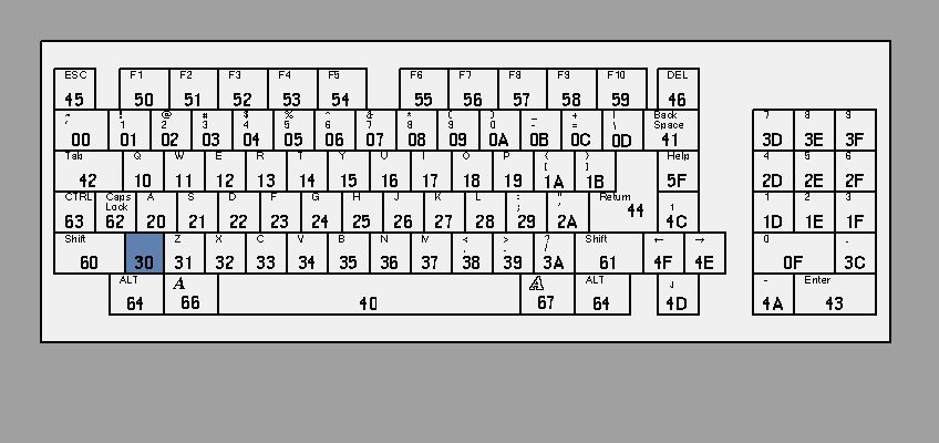
Figure 8-10: The Amiga 1000 Keyboard
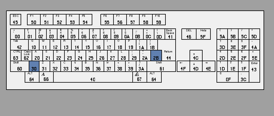
Figure 8-11: The Amiga 500/2000/3000 Keyboard
8 / / Type Of Data Received / RAW Keycodes -> 40-5F hex
Codes common to all keyboards

   40      Space
   41      Backspace
   42      Tab
   43      Numeric Pad "ENTER"
   44      Return
   45      Escape
   46      Delete
   4A      Numeric pad minus
   4C      Cursor up
   4D      Cursor down
   4E      Cursor right
   4F      Cursor left
   50-59   Function keys F1-F10
   5A      Numeric pad left parenthesis
   5B      Numeric pad right parenthesis
   5C      Numeric pad slash "/"
   5D      Numeric pad asterisk
   5E      Numeric pad plus
   5F      Help
8 / / Type Of Data Received / RAW Keycodes -> 60-67 hex
Key codes for qualifier keys

   60      Left Shift
   61      Right Shift
   62      Caps Lock
   63      Control
   64      Left Alt
   65      Right Alt
   66      Left Amiga (or Commodore key)
   67      Right Amiga
8 / / Type Of Data Received / F0-FF hex
These key codes are used for keyboard to 680x0 communication, and are not
associated with a keystroke. They have no key transition flag, and are
therefore described completely by 8-bit codes:

   78      Reset warning.  Ctrl-Amiga-Amiga has been pressed. The
           keyboard will wait a maximum of 10 seconds before
           resetting the machine. (Not available on all keyboard
           models)

   F9      Last key code bad, next key is same code retransmitted

   FA      Keyboard key buffer overflow

   FC      Keyboard self-test fail.  Also, the caps-lock LED will
           blink to indicate the source of the error.  Once for ROM
           failure, twice for RAM failure and three times if the
           watchdog timer fails to function.

   FD      Initiate power-up key stream (for keys held or stuck at
           power on)

   FE      Terminate power-up key stream.

These key codes will usually be filtered out by keyboard drivers.
8 / The Keyboard / Limitations Of The Keyboard
The Amiga keyboard is a matrix of rows and columns with a key switch at
each intersection (see  Appendix G  for a diagram of the matrix). Because
of this, the keyboard is subject to a phenomenon called "phantom
keystrokes." While this is generally not a problem for typing, games may
require several keys be independently held down at once. By examining the
matrix, you can determine which keys may interfere with each other, and
which ones are always safe.

Phantom keystrokes occur when certain combinations of keys pressed are
pressed simultaneously.  For example, hold the "A" and "S" keys down
simultaneously.  Notice that "A" and "S" are transmitted.  While still
holding them down, press "Z".  On the original Amiga 1000 keyboard, both
the "Z" and a ghost "X" would be generated. Starting with the Amiga 500,
the controller was upgraded to notice simple phantom situations like the
one above; instead of generating a ghost, the controller will hold off
sending any character until the matrix has cleared (releasing "A" or "S"
would clear the matrix).  Some high-end Amiga keyboards may implement true
"N-key rollover," where any combination of keys can be detected
simultaneously.

All of the keyboards are designed so that phantoms will not happen during
normal typing, only when unusual key combinations like the one just
described are pressed.  Normally, the keyboard will appear to have "N-key
rollover," which means that you will run out of fingers before generating
a ghost character.

   About the qualifier keys.
   -------------------------
   Seven keys are not part of the matrix, and will never contribute to
   generating phantoms. These keys are:  Ctrl, the two Shift keys, the
   two Amiga keys, and the two Alt keys.
8 Interface Hardware / Serial I/O Interface
A 25-pin connector on the back panel of the computer serves as the general
purpose  serial interface . This connector can drive a wide range of
different peripherals, including an external modem or a serial printer.

For pin connections, see  Appendix E .

 Introduction To Serial Circuitry   Contents Of The Receive Data Register
 Setting The Baud Rate              How Output Data Is Transmitted
 Setting The Receive Mode           Specifying The Register Contents
8 / Serial I/O Interface / Introduction To Serial Circuitry
The Paula custom chip contains a Universal Asynchronous
Receiver/Transmitter, or UART. This UART is programmable for any rate from
110 to over 1,000,000 bits per second.  It can receive or send data with a
programmable length of eight or nine bits.

The UART implementation provides a high degree of software control. The
UART is capable of detecting overrun errors, which occur when some other
system sends in data faster than you remove it from the data-receive
register.  There are also status bits and interrupts for the conditions of
receive buffer full and transmit buffer empty.  An additional status bit
is provided that indicates "all bits have been shifted out". All of these
topics are discussed in folowing sections.
8 / Serial I/O Interface / Setting The Baud Rate
The rate of transmission (the baud rate) is controlled by the contents of
the register named  SERPER .  Bits 14-0 of  SERPER  are the baud-rate
divider bits.

All timing is done on the basis of a "color clock," which is 279.36ns long
on NTSC machines and 281.94ns on PAL machines.  If the  SERPER  divisor is
set to the number N, then N+1 color clocks occur between samples of the
state of the input pin (for receive) or between transmissions of output
bits (for transmit).  Thus  SERPER =(3,579,545/baud)-1. On a PAL machine,
 SERPER =(3,546,895/baud)-1.  For example, the proper  SERPER  value for
9600 baud on an NTSC machine is (3,579,545/9600)-1=371.

With a cable of a reasonable length, the maximum reliable rate is on the
order of 150,000-250,000 bits per second.  Maximum rates will vary between
machines.  At these high rate it is not possible to handle the overhead of
interrupts.  The receiving end will need to be in a tight read loop.
Through the use of low speed control information and high-speed bursts, a
very inexpensive communication network can be built.
8 / Serial I/O Interface / Setting The Receive Mode
The number of bits that are to be received before the system tells you
that the receive register is full may be defined either as eight or nine
(this allows for 8 bit transmission with parity).  In either case, the
receive circuitry expects to see one start bit, eight or nine data bits,
and at least one stop bit.

Receive mode is set by bit 15 of the write-only  SERPER  register. Bit 15
is a 1 if you chose nine data bits for the receive-register full signal,
and a 0 if you chose eight data bits. The normal state of this bit for
most receive applications is a 0.
8 / Serial I/O Interface / Contents Of The Receive Data Register
The serial input data-receive register is 16 bits wide.  It contains the 8
or 9 bit input data and status bits.

The data is received, one bit at a time, into an internal
serial-to-parallel  shift register .  When the proper number of bit times
have elapsed, the contents of this register are transferred to the serial
data read register (SERDATR) shown in Table 8-10, and you are signaled
that there is data ready for you.

Immediately after the transfer of data takes place, the
 receive shift register  again becomes ready to accept new data. After
receiving the receiver-full interrupt, you will have up to one full
character-receive time (8 to 10 bit times) to accept the data and clear
the interrupt. If the interrupt is not cleared in time, the OVERRUN bit is
set.

Table 8-9 shows the definitions of the various bit positions within
SERDATR.

               Table 8-9: SERDATR /  ADKCON  Registers

   SERDATR
   -------

   Bit
   Number  Name    Function
   ------  ----    --------
   15      OVRUN    OVERRUN
                    (Mirror -- also appears in the interrupt request
                    register.) Indicates that another byte of data was
                    received before the previous byte was picked up by the
                    processor.  To prevent this condition, it is necessary
                    to reset INTF_RBF (bit 11, receive-buffer-full) in
                     INTREQ .

   14      RBF      READ BUFFER FULL
                    (Mirror -- also appears in the interrupt request
                    register.) When this bit is 1, there is data ready to
                    be picked up by the processor.  After reading the
                    contents of this data register, you must reset the
                    INTF_RBF bit in  INTREQ  to prevent an overrun.

   13      TBE      TRANSMIT BUFFER EMPTY
                    (Not a mirror -- interrupt occurs when the buffer
                    becomes empty.)  When bit 14 is a 1, the data in the
                    output data register ( SERDAT ) has been transferred to
                    the  serial output shift register , so  SERDAT  is ready
                    to accept another output word.  This is also true when
                    the buffer is empty.

                    This bit is normally used for full-duplex operation.

   12      TSRE     TRANSMIT SHIFT REGISTER EMPTY
                    When this bit is a 1, the  output shift register  has
                    completed its task, all data has been transmitted, and
                    the register is now idle.  If you stop writing data
                    into the output register ( SERDAT ), then this bit will
                    become a 1 after both the word currently in the
                     shift register  and the word placed into  SERDAT  have
                    been transmitted.

                    This bit is normally used for half-duplex operation.

   11      RXD      Direct read of  RXD pin  on Paula chip.

   10               Not used at this time.

   9       STP      Stop bit if 9 data bits are specified for receive.

   8       STP      Stop bit if 8 data bits are specified for receive.
                            OR
           DB8      9th data bit if 9 bits are specified for receive.

   7-0     DB7-DB0  Low 8 data bits of received data.  Data is TRUE (data
                    you read is the same polarity as the data expected).

    ADKCON
   --------

   Bit
   Number  Name     Function
   ------  ----     --------
   15      SET/CLR  Allows setting or clearing individual bits.

                    If bit 15 is a 1 specified bits are set.
                    If bit 15 is a 0 specified bits are cleared.

   11      UARTBRK  Force the transmit pin to zero.
8 / Serial I/O Interface / How Output Data Is Transmitted
You send data out on the transmit lines by writing into the serial data
output register (SERDAT).  This register is write-only.

Data will be sent out at the same rate as you have established for the
read.  Immediately after you write the data into this register, the system
will begin the transmission at the baud rate you selected.

At the start of the operation, this data is transferred from SERDAT into
an internal serial  shift register .  When the transfer to the serial
 shift register  has been completed, SERDAT can accept new data; the TBE
interrupt signals this fact.

Data will be moved out of the  shift register , one bit during each time
interval, starting with the least significant bit. The shifting continues
until all 1 bits have been shifted out. Any number or combination of data
and stop bits may be specified this way.

SERDAT is a 16-bit register that allows you to control the format
(appearance) of the transmitted data. To form a typical data sequence,
such as one start bit, eight data bits, and one stop bit, you write into
SERDAT the contents shown in Figures 8-12 and 8-13.


       15        9 8 7             0
     _________________________________
                                                         |     |
       0 0 0 0 0 0 0 0 0 0 0 0 0 0 0 - - - - - - - - - ->|  1  |
     _________________________________                   |     |

                                                         one bit

                                 All zeros from last shift -


    Figure 8-12: Starting Appearance of SERDAT and Shift Register


                   15        9 8 7                 0
                 __________________________________
                                 |                 |
                   0 0 0 0 0 0 1 |<- 8 bits data ->|
                 ________________|_________________|

                                - - - - - - - - - ->

                     Data gets shfted out this way.


           Figure 8-13: Ending Appearance of Shift Register


The register stops shifting and signals "shift register empty" (TSRE) when
there is a 1 bit present in the bit-shifted-out position and the rest of
the contents of the  shift register  are 0s. When new nonzero contents are
loaded into this register, shifting begins again.
8 / Serial I/O Interface / Specifying The Register Contents
The data to be transmitted is placed in the output register ( SERDAT ).
Above the data bits, 1 bits must be added as stop bits. Normally, either
one or two stop bits are sent.

The transmission of the start bit is independent of the contents of this
register. One start bit is automatically generated before the first data
bit (bit 0) is sent.

Writing this register starts the data transmission. If this register is
written with all zeros, no data transmission is initiated.
8 Interface Hardware / Parallel I/O Interface
The general-purpose bi-directional  parallel interface  is a 25-pin
connector on the back panel of the computer. This connector is generally
used for a parallel printer.

For each data byte written to the parallel port register, the hardware
automatically generates a pulse on the data ready pin.  The acknowledge
pulse from the parallel device is hooked up to an interrupt. For pin
connections and timing, see  Appendix E  and  Appendix F .
8 Interface Hardware / Display Output Connections
All Amigas provide a 23-pin connector on the back.  This jack contains
video outputs and inputs for external genlock devices. Two separate type
of RGB video are available on the connector:

   *  RGB Monitors ("analog RGB"). Provides four outputs; Red (R),
      Green (G), Blue (B), and Sync (S). They can generate up to 4,096
      different colors on-screen simultaneously using the circuitry
      presently available on the Amiga.

   *  Digital RGB Monitors. Provides four outputs, distinct from those
      shown above, named Red (R), Green (G), Blue (B), Half-Intensity
      (I), and Sync (S).  All output levels are logic levels (0 or 1).
      On some monitors these outputs allow up to 15 possible color
      combinations, where the values 0000 and 0001 map to the same
      output value (Half intensity with no color present is the same
      as full intensity, no color). Some monitors arbitrarily map the
      16 combinations to 16 arbitrary colors.

   Note that the sync signals from the Amiga are unbuffered.  For use
   with any device that presents a heavy load on the sync outputs,
   external buffers will be required.

The Amiga 500 and 2000 provide a full-bandwidth monochrome video jack for
use with inexpensive monochrome monitors.  The Amiga colors are combined
into intensities based on the following table:

                       Red     Green   Blue
                       ---     -----   ----
                       30%      60%    10%

The A3000 is not equipped with a monochrome video jack.

The Amiga 1000 provides an RF modulator jack.  An adapter is available
that allows all Amiga models to use a television set for display.  Stereo
sound is available on the jack, but will generally be combined into
monaural sound for the TV set.

The Amiga 1000 provides a color composite video jack.  This is suitable
for recording directly with a VCR, but the output is not broadcast
quality. For use on a monochrome monitor, the color information often has
undesired effects; careful color selection or a modification to the
internal circuitry can improve the results.  The A500, A2000 and A3000 do
not have a color composite video jack. High quality composite adapters for
the A500, A1000, A2000 and A3000 plug into the 23 pin RGB port.

The Amiga 2000 and 3000 provide a special "video slot" that contains many
more signals than are available elsewhere:  all the 23-pin RGB port
signals, the unencoded digital video, light pen, power, audio, colorburst,
pixel switch, sync, clock signals, etc.
Converted on 22 Apr 2000 with RexxDoesAmigaGuide2HTML 2.1 by Michael Ranner.